Ultrapure Water: Transitioning to the 450 mm Wafer Semiconductor Fab
By Jeff Gunderson
Treating raw water to the purity levels required in semiconductor manufacturing demands a robust sequence of advanced processes and water treatment technologies for removing contaminants, minerals, microorganisms, and trace organic and nonorganic chemicals, including other nanoscale particles. Produced ultrapure water (UPW) is utilized in cleaning and etching processes and to wash and rinse semiconductor parts throughout the manufacturing cycle.
As wafer size in semiconductor fabrication has increased over the past decades (from 100 mm in the 1980s and 200 mm in the 1990s to the current 300 mm size), and technology nodes have scaled down to increasingly lower microscopic levels, demand for UPW volume has surged while purity requirements have been driven to the maximum thresholds allowable through technology.
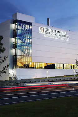
With the industry now setting its sights on the next-generation wafer - the 450 mm computer chip - a first-of-its-kind partnership has been formed at the Colleges of Nanoscale Science and Engineering (CNSE) at the State University of New York (SUNY) Polytechnic Institute to lead the global effort in designing and building the fabrication facilities needed for making this technological leap. The primary objective of the Facilities 450 mm Consortium (F450C) is to enable nanoelectronic fabrication facilities to transition to 450 mm in collaboration with the world’s leading semiconductor facility companies.
Ovivo, the sole water treatment company participating in the consortium, recently completed a state-of-the-art UPW plant expansion at the CNSE facilities that leverages activated carbon filtration, reverse osmosis, ultraviolet irradiation, ion exchange, membrane degasification and microfiltration processes for producing high-level UPW as part of 450 mm research and development.
Lothar Till, managing director at Ovivo Switzerland, said the F450C represents a shared-risk approach for preparing for 450 mm wafer production. “When the industry was ready to move from 200 mm to 300 mm wafer manufacturing, a small group of companies joined together to spearhead the effort and encountered many difficulties and costs,” Till said. “Through joint research and development, the goal of the consortium is to work out solutions to the challenges inherent with this transition and enable companies with the tools for 450 mm production.”
Ovivo’s research efforts at the CNSE are focused on achieving the most efficient water treatment processes and developing solutions that allow for higher recovery UPW systems as well as advanced wastewater reclamation techniques and technologies.
“A semiconductor fab at the 450 mm scale requires a tremendous amount of raw water treated to UPW standards, which is very costly,” Till said. “In order to make this more economical, we are looking at ways to reclaim and recycle UPW wastewater, reducing sewerage costs and the amount of raw water needed.”
Compared to using a city water source, utilizing fab process wastewater to produce UPW may be easier - and more economical - to accomplish, if managed properly, said David Harris, general manager of the electronics and metals division at Ovivo North America.
“Despite it being very contaminated, you typically know what to expect with segregated UPW wastewater,” Harris said. “In contrast, raw water sources can exhibit variability based on seasonal changes, requiring ongoing adjustments throughout the year. As an example, utility water in farming regions can experience periodic spikes in fertilizers and urea, which need to be designed for and treated when detected.”
But while considerable opportunity exists for recycling and reuse in future 450 mm facilities, Till said that the wastewater characteristic of today’s newer and more efficient UPW fab processes is also more problematic to treat.
“In 200 mm production, etching and rinsing operations were traditionally conducted in segregated processes with a dedicated drain system for each, producing waste streams that were less complex and easier to manage,” he said. “But in current-day wafer manufacturing using single-wafer tools, processing occurs in a continuous fashion, generating a cocktail of wastewater in one outfall. Formulating an effective solution requires addressing this combination of different contaminants.”
Right-Sizing and Analytics
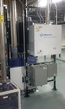
HawsTEC, another partnering member of the F450C, is a company specializing in data analytics that is working with the consortium in right-sizing utilities for future 450 mm fabs. According to HawsTEC, simply scaling existing fabs to accommodate larger wafers could lead to unsustainable construction and operational costs. By employing state-of-the-art monitoring tools in various applications, analytics can be generated to help optimize designs and operational processes.
Initial efforts were focused on monitoring energy use and fluid flows, but the focus has evolved to monitoring effluent streams from process tools to investigate the potential for recovery of used UPW, said Ben Peek, president and CEO of Peek & Associates and a F450C project architect with HawsTEC.
“Understanding the effluent side of semiconductor process tools is becoming more and more important as each step of the semiconductor technology roadmap is achieved,” Peek said. “Today’s state-of-the-art 300 mm fabs use between 2 and 4 million gallons of water per day,” he explained. With the wafer surface area increasing by an order of 2.25 in moving to a 450 mm wafer, water usage could surge to 4.5 to 9 million gallons a day. “When dealing with these volumes of water, even small percentage recoveries are important.”
Finding a location where this amount of water can be reliably supplied presents a challenge and likely constrains the physical location where a fab can be built, Peek added.
HawsTEC’s research with semiconductor effluent includes monitoring the resistivity and pH of rinse cycles to better determine the point at which wastewater is within an acceptable tolerance to be routed back to the front end of an UPW system for reprocessing. Utilizing a highly controlled process system, downstream valves can divert used water in real time, based on changing characteristics.
Heading Toward Higher Purity
Another area of research and development in connection with the F450C includes efforts to produce greater purity UPW that is capable of being effective as a cleaning agent even as wafer technology nodes continue to decrease, pushing the limits of metrology.
“UPW requirements track the technology nodes from the semiconductor technology roadmap,” Peek said. “In moving from 22 nm to a 14 nm width, contaminants become more of an issue and UPW particle size must be substantially smaller than 14 nm to be effective in handling wafer production at this scale.”
As technology nodes progress beyond 14 nm to 10 nm, 7 nm and 5 nm, the amount and purity of required ultrapure water will continue to scale, according to Peek.
“To put this size in perspective, a red blood cell is 2,500 nm in diameter and a strand of DNA is 2.5 nm in diameter,” he said. “At this scale, treatment technology is targeting some really, really small things.”
About the Author: Jeff Gunderson is a correspondent for Industrial WaterWorld. He is a professional writer with over 10 years of experience, specializing in areas connected to water, environment and building, including wastewater, stormwater, infrastructure, natural resources, and sustainable design. He holds a master’s degree in environmental science and engineering from the Colorado School of Mines and a bachelor’s degree in general science from the University of Oregon.


