A new era of semiconductor water management: Challenges, constraints and cutting-edge solutions
Key Highlights
- Digital twins provide a comprehensive, real-time simulation of water systems, enabling proactive decision-making and system optimization across entire fabs.
- AI and advanced analytics are used for predictive maintenance, anomaly detection, and resource optimization, reducing downtime and improving efficiency.
- Innovative treatment technologies, including high-recovery RO, pulse flow systems, and high-pH RO, address scaling and fouling challenges, maximizing water reuse and minimizing waste.
- Zero Liquid Discharge (ZLD) systems, though capital-intensive, are becoming critical in regions with strict discharge regulations, promoting sustainable manufacturing practices.
- The integration of digital and physical innovations will be vital for semiconductor fabs to meet future water demands while reducing environmental footprints.
The global semiconductor market is undergoing a period of unprecedented transformation. Forces that once evolved gradually are now accelerating simultaneously, redefining every aspect of chip production — including one of its most critical resources: water. As microchip fabrication plants (fabs) grow larger, technologies are more complex and environmental expectations more stringent, water systems are being pushed to their limits in both new and existing facilities.
This shift is driven by a convergence of three major pressures:
- Rapidly growing product demand: The rapid rise of generative artificial intelligence (AI) is dramatically increasing the need for memory bandwidth and compute power, fueling global demand for DRAM, logic and advanced packaging capacity.
- A construction boom fueled by the CHIPS Act: Government incentives totaling more than $50 billion for the U.S. semiconductor industry triggered a surge of new fab construction and expansion projects, many of them on a previously unimaginable scale.
- Increasing technological complexity: As chip architectures advance, process water specifications tighten, tool counts rise and wastewater streams diversify. All of these significantly compound the demands placed on fab utilities.
Water supply and waste treatment: The new bottlenecks
These pressures have spawned the era of the mega-fab: sprawling state-of-the-art manufacturing campuses with water needs measured not in millions but in tens of millions of gallons per day. In regions where multiple fabs are clustered — such as greater Phoenix, Arizona — municipal water systems often struggle to keep up with these escalating demands.
On the wastewater side, the challenge is equally acute. Cities must manage sharply increasing loads at Publicly Owned Treatment Works (POTWs), many of which were never designed, hydraulically or chemically, for the complex effluents associated with modern chip manufacturing. Capacity upgrades can lag behind industrial growth by years, creating infrastructure stress for both municipalities and manufacturers.
Regulatory pressure and public expectations
Regulators, investors and communities are also raising the bar. Discharge permits are tightening, pushing plants to adopt more sophisticated treatment trains and advanced polishing steps. At the same time, leading semiconductor companies are setting ambitious sustainability goals to preserve reputation and demonstrate responsible stewardship — especially in water-scarce regions.
The result is a reinforcing cycle: less water available, stricter discharge constraints and rising expectations for internal recycling and reuse.
The need for innovation — and a new way of thinking
Meeting these cumulative challenges requires more than incremental upgrades. It requires a fundamental change in mindset.
Historically, water and wastewater solutions were designed to solve individual issues in isolation — a new tool with a tighter specification, a treatment bottleneck or a permit limit. But this approach overlooks how deeply interconnected fab systems truly are.
This is where digital twins are reshaping the industry.
Seeing the whole water system at once: Digital twins
A digital twin is a high-fidelity, computer-based model of an entire semiconductor water system — from ultrapure water production to reclaim systems, tool discharge, wastewater treatment, site outfall and compliance. By simulating current and future operating conditions, a digital twin enables engineers and managers to:
- Visualize complete water balances (mass and chemistry) across the plant
- Identify reuse options between process areas
- Stress-test water supply and treatment capacity under various production scenarios
- Assess chemical compliance, capacity and scale risks before they occur
- Evaluate the full-plant impact of proposed operational or engineering changes
- Serves as a centralized change management control platform during all phases of project design, construction and operation.
All the above enables decision-makers to act proactively, guided by system-wide insights that are supported by data.
AI in plant operations: Turning data into action
AI and advanced analytics are already part of operations in many modern semiconductor fabs, including their water and utilities systems.
Currently, fabs collect large volumes of sensor data in water and ultrapure water (UPW) systems — flows, conductivities, TOC, pressures, pump status and more. Machine-learning models and data-analytics platforms analyze those data streams in real-time to detect anomalies, forecast maintenance needs and optimize resource consumption.
Current, widely adopted applications include:
- Predictive maintenance: Early detection of membrane fouling, pump or valve degradation, and abnormal operating behavior. This markedly reduces unplanned downtime.
- UPW and reclaim optimization: AI-assisted monitoring of purity metrics are employed to fine-tune dosing, energy use and system performance.
- Smart water tracking: Real-time visualization of water flows and leaks across cooling systems, reclaim units and wastewater treatment areas.
These capabilities help operators maintain high reliability, improve resource efficiency and respond faster to deviations.
Digital twins and AI represent two distinct examples of digital innovation that support the water-management challenges facing today’s semiconductor industry.
Treatment system innovation: Reducing freshwater demand and waste discharge
As industry pushes to maximize water reuse amidst rising demand and the construction of sprawling mega-fabs, the strain on our essential water treatment systems becomes ever more evident.
A software-only strategy, however, is not enough. Achieving substantial gains in water sustainability also requires advances in physical treatment technology. This includes:
- High-recovery reverse osmosis (RO) systems
- Novel polishing technologies for internal reuse
- Selective removal processes for emerging contaminants
- Energy-efficient concentration and brine management systems
The goal is to create plants that use dramatically less freshwater, discharge significantly less waste and continually recycle internal flows at higher purity and efficiency.
In some of the newest semiconductor facilities, traditional municipal support is simply not available. Several emerging fab sites have no access to a POTW, while others face discharge permits so restrictive that meaningful off-site disposal is no longer feasible. In these cases, manufacturers are being pushed toward Zero Liquid Discharge (ZLD) — a condition in which no liquid waste streams leave the site.
ZLD, while environmentally compelling, is one of the most capital- and resource-intensive pathways available. The systems required — thermal concentration units such as evaporators and crystallizers, and large-scale solids handling — represent a significant investment in CAPEX, OPEX and physical footprint. They also demand advanced operational expertise to maintain reliability and energy efficiency.
As a result, minimizing the load sent to the thermal concentration units is a top design priority. This is driving rapid innovation in brine management, with modern approaches focusing on reducing volume and increasing recovery before streams reach the thermal phase. High-recovery RO is becoming an essential tool for shrinking the thermal part boundary while maintaining compliance and maximizing reuse.
RO has become ubiquitous in semiconductor water management, but its widespread adoption brings new problems as we strive for higher recovery rates. When we increase recovery, the ionic concentration in the concentrate stream climbs and salts begin to precipitate on the membrane surface, overwhelming the capacity of added antiscalants (scale inhibitors) and blocking membrane pores with intensive scaling.
Left unchecked, supersaturation in the last elements of a pressure vessel will exceed the antiscalant’s protective envelope, and scaling will build up. Meanwhile, residual total organic carbon (TOC), biochemical oxygen demand (BOD) and chemical oxygen demand (COD), in combination with bacteria, conspire to form biofilms on the membrane, restricting flow. The higher the permeate flux, the more aggressively these microbes colonize the first elements in the pressure vessel. Another by-product of chasing high recovery is low brine flow: with less concentrate flow, shear forces drop, causing more ions to accumulate at the membrane surface, thus accelerating scaling once again.
All these mechanisms conspire to clog pores, sap membrane permeability and drive up energy consumption. Restoring performance demands cleaning the membranes, usually through clean-in-place (CIP), a procedure that incurs downtime, extra costs and the gradual attrition of membrane life. In the worst cases, the damage is irreversible, and the only remedy is to replace the fouled elements.
To meet these challenges head on, the high-recovery reverse osmosis (HRRO) field has given rise to an intriguing family of innovations: pulse flow RO (PFRO), closed circuit RO (CCRO), flow reversal RO (FR-RO), MaxH2O Desalter and high-pH RO. Each technology surpasses the recovery attainable in a conventional RO train by tackling scaling and fouling with different processes/mechanisms. Regard the approach to solve the scaling problem they fall loosely into two camps: those that work without removing sparingly soluble salts, and those that remove them from the equation altogether.
Manipulations of flow dynamics
In the first camp, designers play with the flow itself. By periodically reversing the flow direction or snapping a brine valve fully open for a short interval, the system resets the physical conditions before crystals can take hold. Crystal formation follows induction, nucleation and growth; the clever timing in PFRO, CCRO and FR-RO — switching every few seconds or minutes, depending on the technology — interrupts the induction period and keeps supersaturation from ever progressing to actual scaling. Early in a cycle, the pressure vessel sees feed-strength water, and at the end it might see salinities ten times higher; the constant swing makes it difficult for bacteria to reproduce, since microbes expend energy merely adapting to shifting conditions instead of building a biofilm. For example, one of the technologies mentioned, the PFRO, the intentional opening of the brine valve boosts crossflow velocity and shear at the membrane surface, aiding in autogenous cleaning. To buffer the rest of the plant from abrupt flow changes, systems are partitioned into groups of pressure vessels so that only one subset is in its flushing interval at a time. PFRO even permits cleaning in operation (CIO) — as opposed to traditional CIP — by isolating and servicing a group on the fly and recycling the cleaning liquor, which trims chemical use and significantly extends the periods between full CIPs.
Figures 2 a-c show real data of a PFRO system running in a fab for several months without CIP, compared to a conventional RO system running with the same water, but works at lower water recovery and still must undergo CIP once a week to return to the same levels of production.


These non-salt-removing techniques deliver a tangible performance lift compared with conventional RO, but they encounter a ceiling: once the effluent leaves the system, supersaturation can still occur in the downstream piping, if the conditions are too extreme, and scaling sets outside of the controlled environment. Moreover, when we continue elevating the water reclaim percentage higher, even this unique system will not be able to sustain the unavoidable oversaturation of salts eventually results in heavy scaling on the membrane surface. That residual risk caps the maximum recovery that can reasonably be pushed in the field.
Manipulations of supersaturation conditions: pH change, removal of ions/salts from the water
The second category takes a more aggressive approach: it removes the sparingly soluble species that seed trouble in the first place. Desalters and high-pH RO packages induce ion removal, so that troublesome components drop out before they ever contact the next membrane stage. High-pH RO accomplishes this with an ion exchange (IX) unit followed by a degasifier, that softens the feed of calcium and carbonate and enables operation at high pH where silica scaling is muted, and organic fouling risk is reduced. The trade-off is the need for extra capital and operating expenses, a larger footprint and an additional waste stream from the IX regeneration that must be responsibly managed.
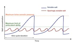
The novel Desalter approach harnesses a fluidized bed reactor (FBR) to nucleate sparingly soluble salts. The up flow through a vertical cylinder floats the seeds, enabling heterogeneous precipitation across a huge surface area, while maintaining the concentration of the sparingly soluble salts below the antiscalant limit. The above mentioned is demonstrated well in Figure 3.
The vertical design decreases the footprint, and the heterogeneous precipitation trims chemical consumption. The by-product is a dry pellet, which can reach up to 90% DS without any dewatering equipment — only natural evaporation inside a silo with screen. Then, it can be conveniently discharged and disposed of. The Desalter also enjoys the advantages of high brine flow which improves shear and cyclic salinity modulation, both combined are discouraging microbial settlement and reduce scaling.
Conclusion
Looking ahead toward 2026 and beyond, addressing these challenges will be pivotal for the semiconductor industry’s sustainability: Mastering high-recovery RO, innovative polishing and brine management, and next-generation technologies such as PFRO, CCRO, FR-RO, Desalter and high efficiency RO will enable fabs to pursue near-ZLD without sacrificing throughput or reliability. As the market scales, broader adoption of these inventive HRRO technologies integrated with advanced sensors, digital twins and AI will allow real-time tuning of operations. With reduced energy bills, lower chemical consumption and a shrunken environmental footprint, the promise of sustainable semiconductor manufacturing is within reach, empowering designers and operators alike to build the water-wise fabs that our thirsty world demands.